

Researchers at MIT and other institutions have found a way to grow a fragile, atom-thin superconducting material in large, uniform sheets that do not degrade when exposed to air, a problem that has blocked practical use of these materials for years.
The material is called niobium diselenide. It consists of a single tightly packed layer of niobium atoms sandwiched between two layers of selenium atoms. At just one or a few atoms thick, it belongs to a class of two-dimensional superconductors that can conduct electricity with zero resistance despite their extreme thinness. That combination of tiny size and powerful electrical properties has made them attractive candidates for shrinking quantum computing hardware, but until now they were nearly impossible to work with outside of a controlled laboratory setting.
The reason is oxidation. Exposed to open air, these ultrathin materials break down rapidly. Earlier methods could only produce them in very small patches, making large-scale manufacturing impossible.
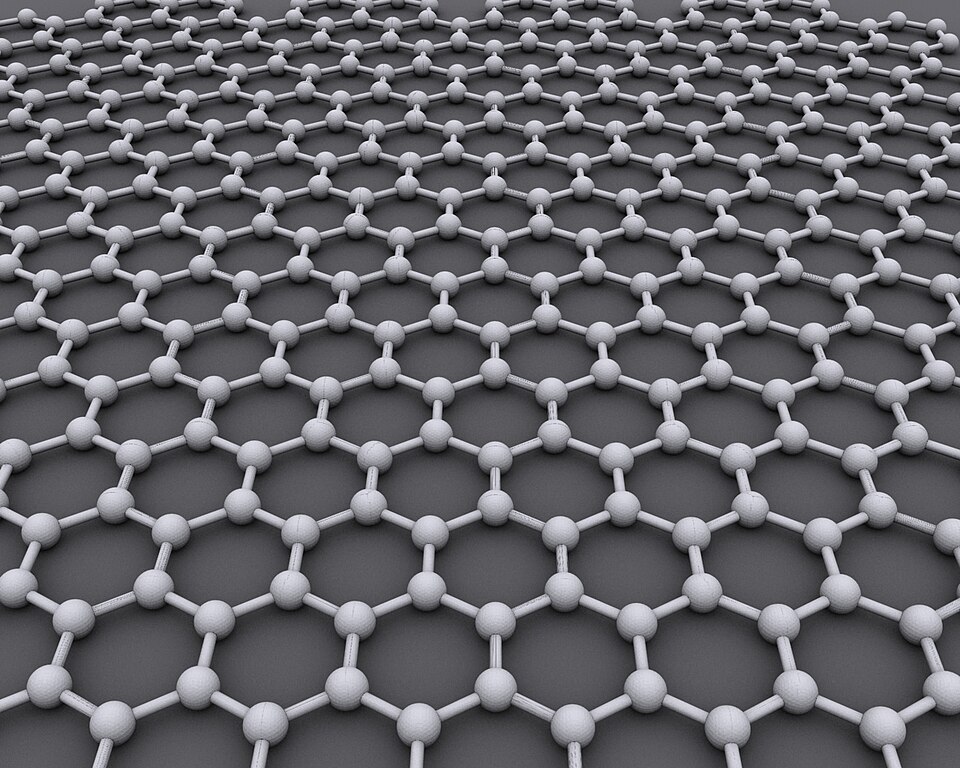
The MIT-led team solved the problem by growing the niobium diselenide underneath a layer of graphene, an atomically thin carbon material. The graphene acts as a protective cap, shielding the superconductor from the oxygen and moisture that would otherwise destroy it. At the same time, the graphene guides the superconductor to form a smooth, even layer across a surface the size of a full semiconductor wafer, according to a report by Phys.org.
After growing the material, the researchers integrated it into a superconducting microwave circuit and tested it. The niobium diselenide held its superconducting properties and showed high kinetic inductance, a measure of how much inductive energy a material can store in a small area. High kinetic inductance in a compact form is a desirable trait in many quantum devices.
Currently, engineers who want large kinetic inductance in a quantum circuit typically build long chains of devices called Josephson junctions, which take up significant space. A material like niobium diselenide with naturally high kinetic inductance could replace those arrays, making circuits smaller and simpler.
"Emerging superconductors that are only a monolayer thick have a lot of potential. Thanks to our new process, they are no longer materials that can only be made at a very small scale. There are now exciting opportunities for scientists to study these materials, use them in circuits, and explore their practical applications," said co-lead author Xudong Sheldon Zheng, a graduate student in MIT's Department of Electrical Engineering and Computer Science.
Beyond quantum computing, the researchers say the advance could benefit ultrasensitive quantum detectors used in communications and cosmology. The findings were published in the journal Nature.